|
 |
|
A fast bio-nanotechnology platform to
capture/detect bacteria in clinical samples
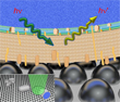
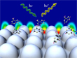
Detecting bacteria in clinical samples without using time-consuming culture processes would allow rapid diagnoses. Such a culture-free detection method requires the capture and analysis of bacteria from a body fluid, which are usually of complicated composition. This team has shown that coating Ag-nanoparticle arrays with vancomycin (Van) can provide label-free analysis of bacteria via SERS, leading to a ~1,000-fold increase in bacteria capture, without introducing significant spectral interference. Bacteria from human blood can be concentrated onto a designated minuscule Van-coated area while blood cells are excluded. Furthermore, such Van-coated substrate produces noticeably distinct SERS spectra of Van-susceptible and Van-resistant Enterococcus, indicating its potential use for drug-resistance tests. This SERS-based in situ detection method provides a good opportunity to help solve the prob-lem faced by conventional biological assays that commonly require a sample preparation time ranging from days for fast growing bacteria to weeks for slow growers. The results represent a critical step towards the creation of SERS-based multifunctional biochips for rapid culture- and label-free detection and drug-resistant testing of microorganisms in clinical samples.
More
details  Full
text : [PDF
] Full
text : [PDF
] |
|
|
|
|
|
|
|
|
|
|
|
|
|
|
|
|
|
|
|
 |
|
Looking into Meta-Atoms of Plasmonic Nanowire Metamaterial
Nanowire-based plasmonic metamaterials exhibit many intriguing properties related to the hyperbolic dispersion, negative refraction, epsilon-near-zero behavior, strong Purcell effect, and nonlinearities. We have experimentally and numerically studied the electromagnetic modes of individual nanowires (meta-atoms) forming the metamaterial. High-resolution, scattering-type near-field optical microscopy has been used to visualize the intensity and phase of the modes. Numerical and analytical modeling of the mode structure is in agreement with the experimental observations and indicates the presence of the nonlocal response associated with cylindrical surface plasmons of nanowires.
More
details Full
text : [PDF
] |
|
|
|
|
|
|
|
|
|
|
|
|
|
|
|
|
|
|
|
 |
|
Custom-designed arrays of anodic alumina nanochannels with individually tunable pore sizes
We demonstrate a process to selectively tune the pore size of an individual nanochannel in an array of high-aspect-ratio anodic aluminum oxide (AAO) nanochannels in which the pore sizes were originally uniform. This novel process enables us to fabricate arrays of AAO nanochannels of variable sizes arranged in any custom-designed geometry. The process is based on our ability to selectively close an individual nanochannel in an array by using focused ion beam (FIB) sputtering, which leads to redeposition of the sputtered material and closure of the nanochannel with a capping layer of a thickness depending on the energy of the FIB. When such a partially capped array is etched in acid, the capping layers are dissolved after different time delays due to their different thicknesses, which results in differences in the time required for the following pore-widening etching processes and therefore creates an array of nanochannels with variable pore sizes. The ability to fabricate such AAO templates with high-aspect-ratio nanochannels of tunable sizes arranged in a custom-designed geometry paves the way for the creation of nanophotonic and nanoelectronic devices.
More
details Full
text : [PDF
] |
|
|
|
|
|
|
|
|
|
|
|
|
|
|
|
|
|
|
|
 |
|
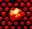
Stepwise self-assembly of C60 mediated by atomic scale moire magnifiers
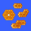
Self-assembly of atoms or molecules on a crystal surface is considered one of the most promising methods to create molecular devices. Here we report a stepwise self-assembly of C60 molecules into islands with unusual shapes and preferred sizes on a gold–indium-covered Si(111) surface. Specifically, 19-mer islands prefer a non-compact boomerang shape, whereas hexagonal 37-mer islands exhibit extraordinarily enhanced stability and abundance. The stepwise self-assembly is mediated by the moire interference between an island with its underlying lattice, which essentially maps out the adsorption-energy landscape of a C60 on different positions of the surface with a lateral magnification factor and dictates the probability for the subsequent attachment of C60 to an island’s periphery. Our discovery suggests a new method for exploiting the moire interference to dynamically assist the self-assembly of particles and provides an unexplored tactic of engineering atomic scale moire magnifiers to facilitate the growth of monodispersed mesoscopic structures.
More
details Full
text : [PDF
] |
|
|
|
|
|
|
|
|
|
|
|
|
|
|
|
|
|
|
|
 |
|
On-Chip Thin Film Zernike Phase Plate for In-Focus Transmission Electron Microscopy Imaging of Organic Materials
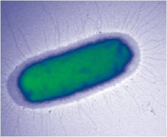
Transmission electron microscopy (TEM) is a powerful tool for imaging nanostructures, yet its capability is limited with respect to the imaging of organic materials because of the intrinsic low contrast problem. TEM phase plates have been in development for decades, yet a reliable phase plate technique has not been available because the performance of TEM phase plates deteriorates too quickly. Such an obstacle prohibits in-focus TEM phase imaging to be routinely achievable, thus limiting the technique being used in practical applications. Here we present an on-chip thin film Zernike phase plate which can effectively release charging and allow reliable in-focus TEM images of organic materials with enhanced contrast to be routinely obtained. With this stable system, we were able to characterize many polymer solar cell specimens and consequently identified and verified the existence of an unexpected nanoparticle phase. Furthermore, we were also able to observe the fine structures of an Escherichia coli specimen, without staining, using this on-chip thin film phase plate. Our system, which can be installed on a commercial TEM, opens up exciting possibilities for TEM to characterize organic materials.
More
details Full
text : [PDF
] |
|
|
|
|
|
|
|
|
|
|
|
|
|
|
|
|
|
|
|
 |
|
AAO nanochannels reshaped into vertical fan-out platform
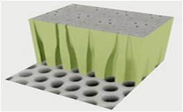
Focused ion beam lithography and a two-step anodization have been combined to fabricate a vertical fan-out platform containing an array of unique probes. Each probe comprises three anodic alumina nanochannels with a fan-out arrangement. The lithography is used to pattern an aluminum sheet with a custom-designed array of triangular 'cells' whose apexes are composed of nanoholes. The nanoholes grow into straight nanochannels under proper voltage in the first-step anodization. The second step uses a doubled voltage to induce lateral repulsion among the nanochannels' growth fronts originating in the same cell. Therefore, the fronts fan out. The repulsion roots in the inter-front distance being shorter than the naturally favoured length, which increases with anodization voltage. The fan-out evolution continues until the growth fronts originating in all the cells evolve into a close-packed two-dimensional hexagonal lattice whose spacing is identical to the favoured one. The chemical and physical mechanisms behind the fan-out fabrication are discussed. This novel fan-out platform facilitates probing and handling of many signals from different areas on a sample's surface and is therefore promising for applications in detection and manipulation at the nanoscale level.
More
details Full
text : [PDF
] |
|
|
|
|
|
|
|
|
|
|
|
|
|
|
|
|
|
|
|
 |
|
Topological Solitons Break Even/Odd Symmetry in Picking Particle's Distances
Depositing particles randomly onto a one-dimensional lattice is expected to result in equal number of particle-pairs separated by even or odd lattice units. However, such even/odd symmetry is broken in the self-selection of distances between indium magic-number clusters on a Si(100)-2x1 reconstructed surface. Cluster-pairs separated by even lattice units are less abundant because they are linked by two silicon atomic chains carrying topological solitons that induces local strain and create localized electronic states with higher energy. The finding reveals a unique particle-particle interaction mediated by the presence or absence of topological solitons on alternate lattices.
More
details Full
text : [PDF
] |
|
|
|
|
|
|
|
|
|
|
|
|
|
|
|
|
|
|
|
 |
|
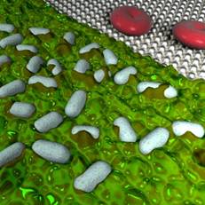
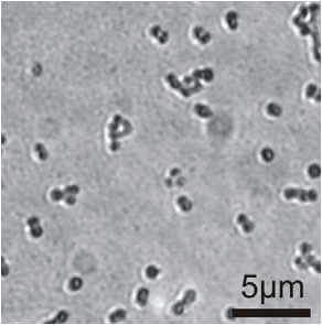
Transparent Raman-enhancing substrates for microbiological monitoring and in situ pollutant detection
Opaque Raman-enhancing substrates made of Ag nanoparticles on incompletely oxidized aluminum templates have been rendered transparent by an ion-drift process to complete the oxidation. The result shows that the transparent substrates exhibit high/uniform surface-enhanced Raman scattering (SERS) capability and good optical transmissivity, allowing for concurrent SERS characterization and high contrast transmission-mode optical imaging of S. aureus bacteria. We also demonstrate that the transparent substrates can used in conjunction with optical fibers as SERS sensors for in situ detection of malachite green down to 10?9 M.
More
details Full
text : [PDF
] |
|
|
|
|
|
|
|
|
|
|
|
|
|
|
|
|
|
|
|
 |
|
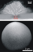
Dendritic structure grown from a single isolated anodic alumina nanochannel
Porous anodic aluminum oxide (AAO) membranes have been widely used as templates for growing nanomaterials because of their ordered nanochannel arrays with high aspect ratio and uniform pore diameter. However, the intrinsic growth behavior of an individual AAO nanochannel has never been carefully studied for the lack of a means to fabricate a single isolated anodic alumina nanochannel (SIAAN). In this study, we develop a lithographic method to fabricate the first SIAAN. The cross-sectional TEM image reveals a dendritic structure grown from a SIAAN, as indicated in the red rectangle. Later, the SIAAN starts to branch randomly and forms a highly ramified dendritic structure with a very rough growth front. For a longer anodization time, such dendritic pores grow simultaneously into a smooth hemispherical growth front. The SEM image shows a fully developed hemispherical porous structure with its barrier (capping) layer removed by etching, which reveals the pores with approximately polygonal close-packing arrangement on the growth front. The study provides an overview of the evolution from single to multiple nanochannels and also reveals an AAO nanochannel has branching nature which is characteristically different from that of the well-known straight arrayed nanochannels formed by anodizing a flat aluminum surface.
More
details Full
text : [PDF
] |
|
|
|
|
|
|
|
|
|
|
|
|
|
|
|
|
|
|
|
 |
|
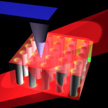
Imaging visible light using anisotropic metamaterial slab lens
It has been shown that an anisotropic metamaterial made of nanowire array can realize negative refraction of light even without a negative phase index of refraction. Such non-resonant bulk material can be fabricated by bottom-up electrochemical method. Using this material, we were able to achieve lensing action with micron-thick slab and demonstrate imaging of a slit object. The details of the focused light beam in 3-dimensional space have been mapped with near field scanning optical microscope (NSOM).
More
details Full
text : [PDF] |
|
|
|
|
|
|
|
|
|
|
|
|
|
|
|
|
|
|
|
 |
|
High-speed Detection and Identification of Bacteria Using Raman enhancing substrate
The surface-enhanced Raman scattering (SERS) technique based on Ag nanoparticles SERS-active substrate was applied to assess the fine structures of the bacterial cell wall. The SERS profiles recorded by such technique are sensitive and stable, that could readily reflect different bacterial cell walls found in Gram-positive, Gram-negative, or mycobacteria groups. The characteristic changes in SERS profile were noticed in the drug-sensitive bacteria at the early period (i.e., ~1 hr) of antibiotic exposure, which could be used to differentiate them from the drug-resistant ones. The high-speed SERS detection represents a novel approach for microbial diagnostics.
More
details Full
text : [PDF
] |
|
|
|
|
|
|
|
|
|
|
|
|
|
|
|
|
|
|
|
 |
|
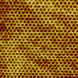
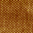
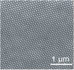
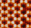
Highly Raman Enhancing Substrates Made of Ag-Nanoparticle Array with Tunable Sub-10 nm Gaps
Substrates with extremely high surface-enhanced Raman scattering (SERS) activity are fabricated based on arrays of Ag-nanoparticles on the surface of anodic aluminum oxide (AAO) film. The gaps between the Ag-nanoparticles are precisely varied in the unprecedented sub-10-nm scale and the SERS enhancing power increases dramatically with the narrowing of the gaps. The results provide quantitative evidence of collective SERS effect and confirm predictions of interparticle-coupling induced Raman enhancement. The Raman enhancing substrate's uniform and highly reproducible SERS-active properties as well as its wide dynamical range facilitate the use of SERS for many chemical/biological sensing applications.
More
details Full
text : [PDF
] |
|
|
|
|
|
|
|
|
|
|
|
|
|
|
|
|
|
|
|
 |
|
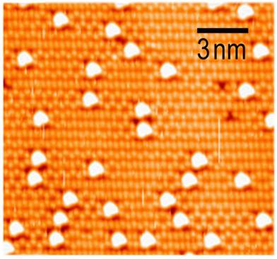
Surface Magic
Cluster (SMC) and its lattices
Under certain deposition
conditions, gallium induces almost exclusive formation of a type
of especially stable clusters --- magic clusters, on the 7 x 7-reconstructed
silicon (111) surface. The cluster has a triangular closed-shell
structure and resides on the center of a 7 x 7 half unit-cell. As
the gallium coverage is increased, the cluster density increases
proportionally, leading essentially to the complete filling of the
7 x 7 half unit-cells and the creation of an unprecedented two-dimensional
lattice of magic clusters. A structure model employing three silicon
atoms to link six gallium atoms into a configuration with satisfied
bonding is proposed to qualitatively account for the cluster's stability.
More
details Full
text : [PDF
] |
|
|
|
|
|
|
 |
|
|
|
|
|
|
|
|
|
|
|
|
|
|
Ordered anodic
alumina nanochannels on focused-ion-beam-prepatterned aluminum surfaces
A combined process of
electropolishing, focused-ion-beam lithography, and controlled anodization
is used to fabricate anodic alumina films with ordered nanochannels.
The ion beam is used to create a hexagonally close-packed lattice
of concaves on a polished aluminum surface and the concaves act
as pinning points for guiding the growth of nanochannels in the
following anodization step. By carefully matching the lattice constant
(100 nm) with the anodization voltage, ordered nanochannels with
aspect ratio of ~100 are fabricated. The effects of the ion dose
and its corresponding depth of the concaves on the ordering of the
nanochannel array are investigated and a minimum depth of 3 nm is
found to be necessary for effective guidance of the growth of ordered
nanochannels.
More
details Full
text : [PDF
] |
|
|
|
|
|
|
|
|
|
|
|
|
|
|
|
|
|
|
|
|
|
|
|
|
|
|
|
|